Table of Contents
Class D audio amplifier
Description
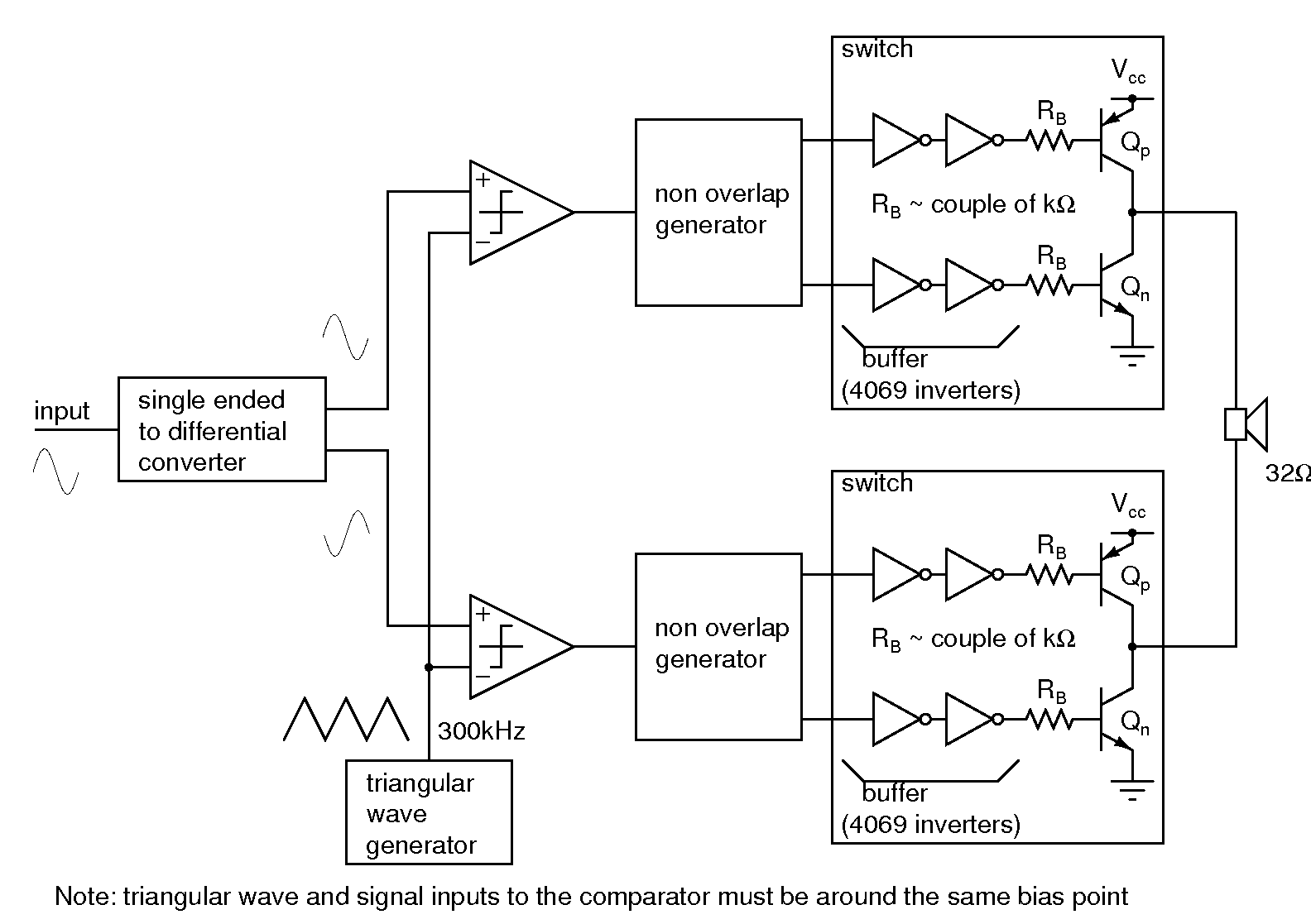
A class D audio amplifier is a pulse width modulator followed by a switch that will drive the speakers. Normally one needs filters at the output to remove the high frequency components. In addition to removing the high frequency components, the filter also improves the efficiency by minimizing the high frequency signal across the load. (e.g. A pulse width modulator with zero input outputs a 50% duty cycle square wave. Even if we can't hear this, power is dissipated when it is applied across the load). In case of audio, the ear filters out the high frequency signals. Good efficiency can be obtained from what is known as a “bridged three level topology”. For details, see references below. The idea is to operate two pulse width modulators with inputs of opposite phases. The load is connected differentially between the two switches. It is easy to see that, for zero input, both sides produce the same 50% duty cycle square wave and the voltage across the load, and hence the power dissipation, is zero, whereas, with a single switch, without a filter, a power of Vcc2/2RL would have been dissipated.
Block diagram and specifications
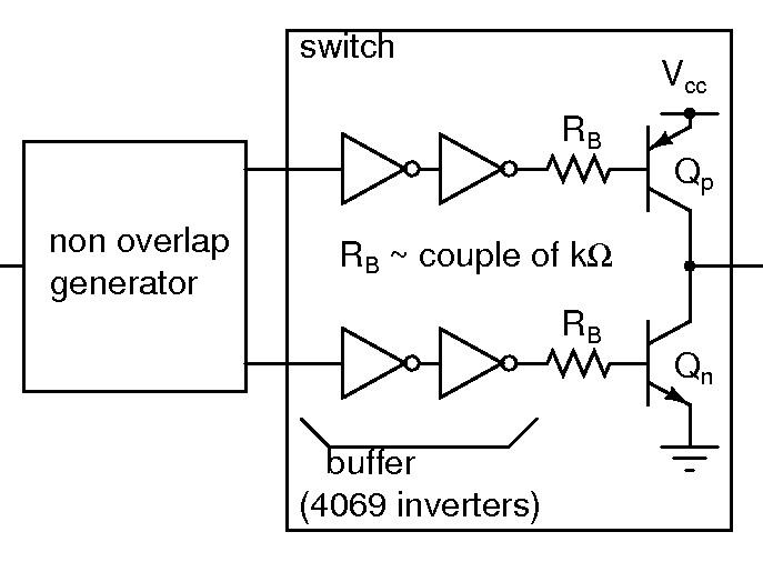
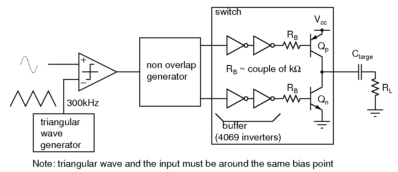
The bridged three level class D amplifier is shown above. To generate the inverted waveform from the input, an amplifier of gain -1 is used. Two identical pulse width modulators are used. A 300kHz triangular wave is used for pulse width modulation. Qp and Qn are the output switches. They are driven by CD4069 inverters into saturation(“ON”) or cutoff(“OFF”). If Qp and Qn are turned on simultaneously, there will be a short circuit between the supply and ground and a large amount of current will be drawn. To prevent this, there should be a nonoverlap between the ON periods of Qp and Qn. A nonoverlap generator is used to achieve this.
Implement the entire amplifier with a single 5V supply.
Pulse width modulator
Use LM311 comparator for the pulse width modulator. Refer to this page for details.
Oscillator
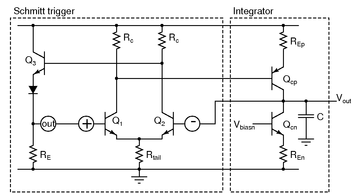
The oscillator is based on the same principle as the one in the experiment done previously. But, a 300kHz triangular wave oscillator cannot be made using LF347 opamps, which have a gain bandwidth product of 4MHz. Therefore, the schmitt trigger and integrator are made using transistors.
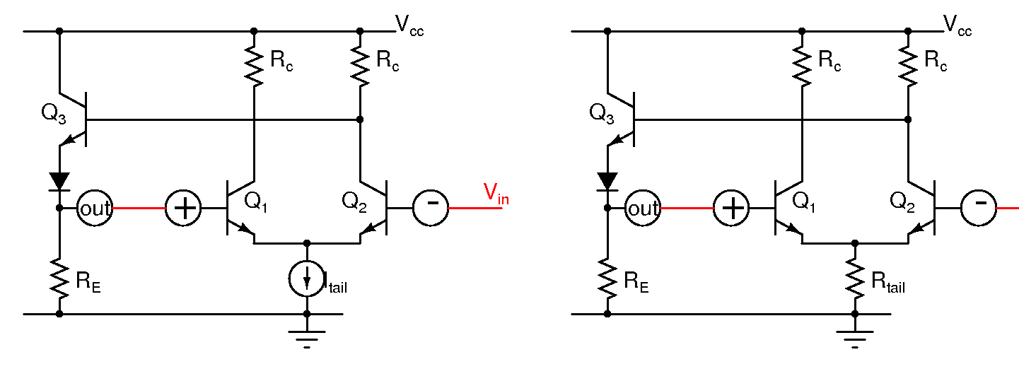
The schmitt trigger is shown above. The opamp(differential pair + emitter follower) is placed in unity positive feedback. The diode provides an extra 0.7V level shift which increases the possible signal swing. Choose Itail and Rc to realize the largest swing without driving the transistors into saturation.
The schmitt trigger drives an integrator and the integrator's output in turn drives the schmitt trigger. Qcp and REp form the upper current source and Vbiasn, Qcn and REn form the lower current source. The former is switched on and off by the schmitt trigger and the later is always on. Adjust the values such that equal currents flow into or out of the capacitor in the two phases. Adjust the current and capacitor values to obtain the desired frequency.
Non overlap generator
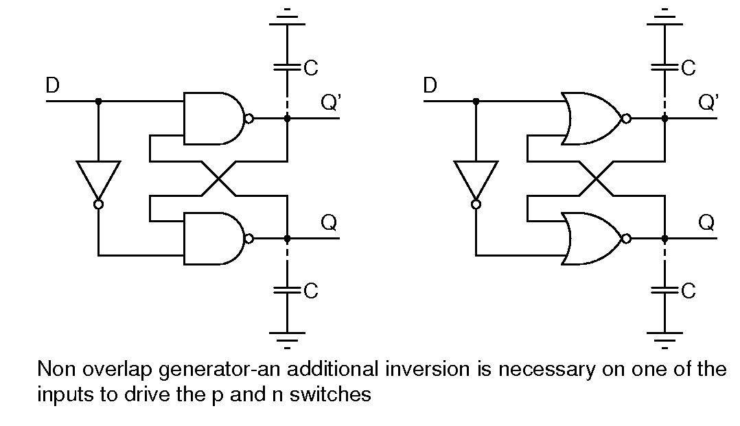
As mentioned before Qp and Qn in the class D amplifier must be switched so that they are never ON simultaneously. Otherwise, besides reduced efficiency, the transistors may blow because of overheating. This means that the “low” period at the base of Qp and the “high” period at the base of Qn should be nonoverlapping.
The circuits above generate complementary waveforms with nonoverlapping high or low periods. Adjust the additional loading capacitor to obtain a nonoverlap period which is a few percent of the total period. Use one of these with an appropriately placed additional inversion stage so that when the input is high, Qp is switched on, when the input is low, Qn is switched on, and there is nonoverlap between the two ON periods.
Switch
The switch is the output stage of the class D amplifier and is the key to obtaining good efficiency. In this project, implement them with NPN and PNP transistors and drive them with CMOS inverter buffers. Start with a base resistance(bases of Qp and Qn) of a few kilohms to limit the base current. If you find that the drive is insufficient(i.e. the transistors don't saturate with a heavy load), reduce the base resistances so that they saturate. If you find that the drive is still not sufficient, you can omit the base resistor, and connect two inverters in parallel to drive the base of the transistors.
Generating the inverted version of the input
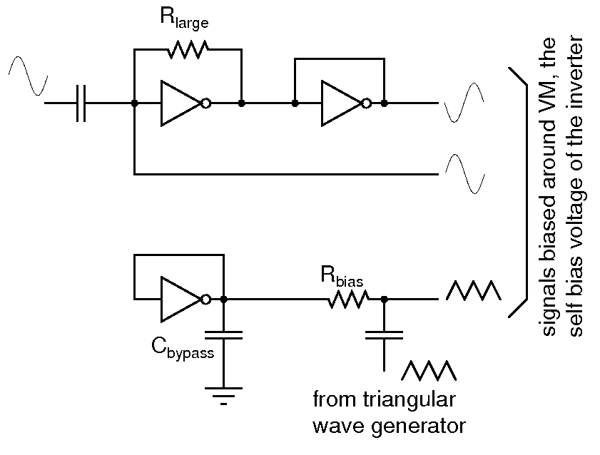
You can use the simple circuit above using CMOS inverters to invert the input. The two waveforms will be biased around the self bias voltage of the inverter. For proper operation, the input signals and the triangular wave should have the same dc level. For this, ac couple the triangular wave and set the dc bias using a self biased inverter as shown above.
How to go about building it
One of you can work on the triangular wave oscillator and the other on the nonoverlap generator and the switch. Once both are tested individually, make the circuitry to get differential inputs and add dc bias to the triangular wave. Put together the single ended circuit shown below, also known as the “half bridge” and test it. In this case, it is essential that you ac couple the load.
Once this is successfully verified, duplicate the switch and the nonoverlap generator and drive it with the inverted output. Verify the second half by itself as before. Once both halves are working as expected, connect the load between them.
Precautions:
- Once you power it up, touch the transistors and ensure they aren't overheating.
- The metal transistor case is connected to the collector. So make sure transistor's don't touch other transistors or component leads.
- Always test the switch with a high impedance load(~1kΩ) first. Then substitute a low resistance(~22Ω).
- Connect the speaker to the final circuit only after the TAs have inspected the circuit and ensured that it is properly functional.
References
- Class D Audio amplifiers-Self study course, Aug.-Dec. 2008: See the list of references at this link.
