PCB Design Software Tutorial
PCB is a free software tool for the UNIX operating system that is used
to lay out printed-circuit boards. PCB does not, however, include
a tool for creating circuit schematics. Because the PCBs we will
design have a relatively small number of components, we will forgo the
latter step and just build the layout directly.
To load PCB, at the command prompt type:
/tools1/pcb/bin/pcb
This will bring up the PCB interface. Before starting your
layout, read chapters 1-3 and 8 from the user guide. This will
familiarize you with some of the basic commands and techniques using
the software. The manual can be found at:
/tools1/pcb/share/pcb/pcb.pdf
In addition, an example pcb layout can be found in
/tools1/pcb/share/pcb/tutorial/tut1.pcb
You can use this to experiment with the software before beginning your
own layout.
Designing Your Own PCB
The following tutorial will allow you to become better acquainted with
the PCB software.
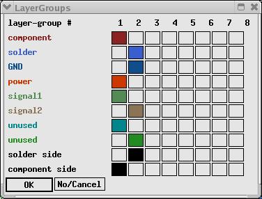
1. We will be designing a two-layer PCB only. Therefore,
specify the layers as shown in the figure below. Do this by
selecting Settings -> Edit
layer groupings from the top menu. We will assume that all power
lines will be routed on the top (component side) of the board, while
GND wires and planes will be present on the bottom (solder side).
2. Set the board size by selecting Edit -> Change board size.
Set the PCB width and height to 6000.00 and 3000.00,
respectively. This size should be sufficient for your
board. Note that all measurements are in units of "mils" (0.001
in.).
3. Set the zoom setting in the Screen
menu to 1:2 and select Display grid.
Also change the grid setting to 1 mil.
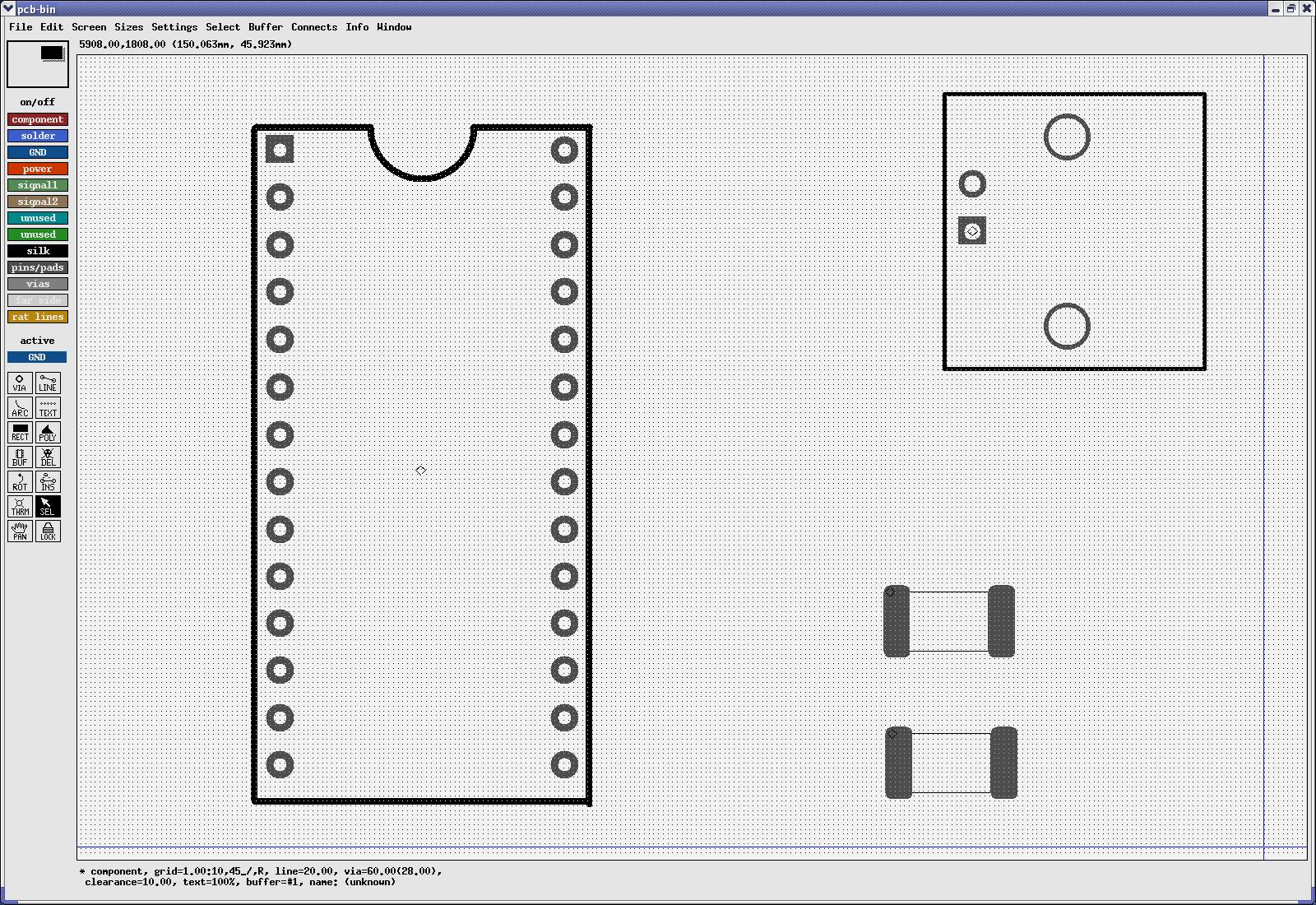
4. We will now place a few component "footprints" on the board
and wire them up. A footprint contains all the pads on which a
real component will sit. We will use BNC connectors to route
power and GND signals. Go to the ~connector group in the PCB
library menu and select the "1, right angle BNC" component. Place
it anywhere in the layout. Now obtain the MOSIS_DIP28_ele component by
accessing File -> Load element
data to paste-buffer and then selecting the directory where this
component resides. Place this near the DIP connector. Note
that these components are known as "through-hole" because their pins
physically pass through the PCB.
5. Go to the ~genericsmt
library and select the "6400, 3200, 750, SMT type capacitor/resistor"
footprint. Place two of these on the board. This footprint
is known as a "surface-mount" component because it contains pins that
sit on the top (or bottom) surface of the PCB. Arrange the
components so that they look similar to the figure shown below.
6. Now we must name each of the components in our layout.
Select the BNC connector, click the right mouse button, and then choose
Edit Name from the list.
Name the connector "BNC1". You will see this name appear on the
footprint. Name the DIP package "IC", and the top and bottom
resistors "RES1" and "RES2", respectively.
7. To view the pin numbers of each component, select the
component and hit "<Esc>D". You may have to zoom in to see
these better.
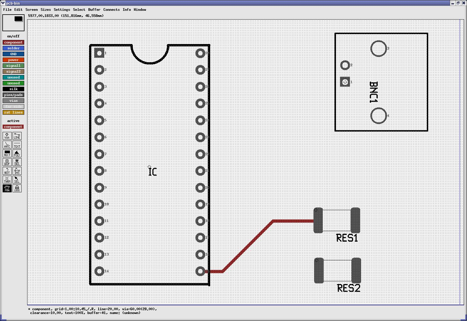
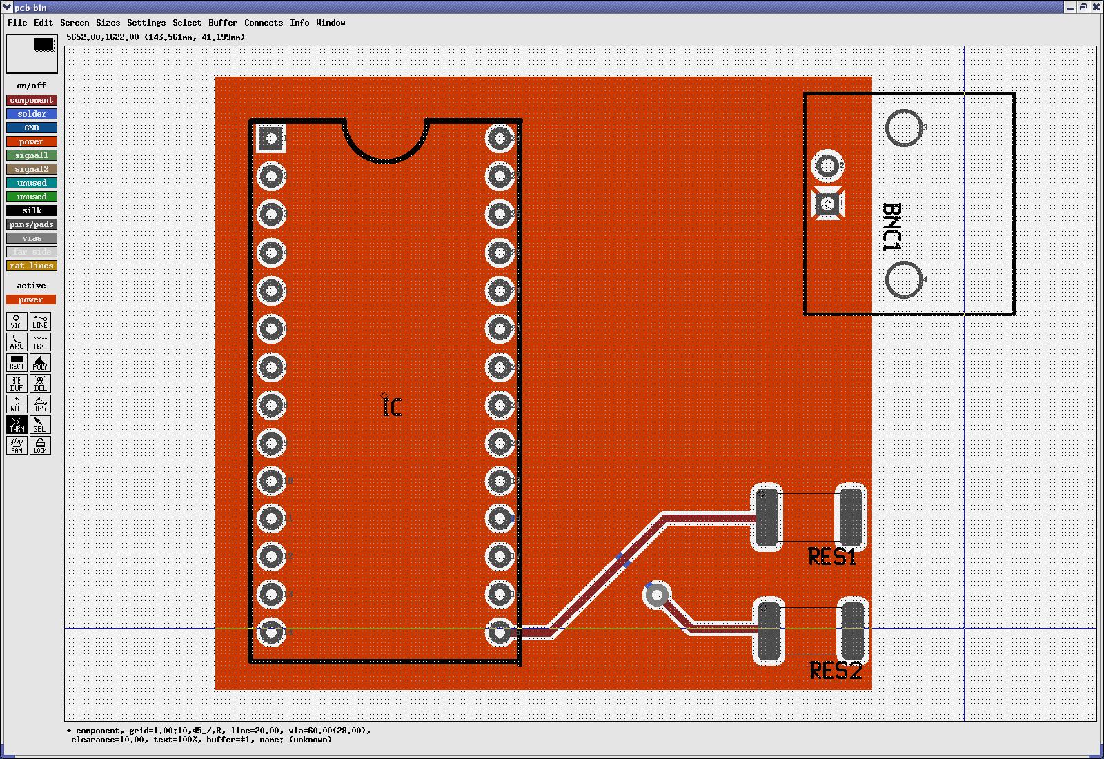
8. Before we begin drawing the wires, select Sizes and increase the line width
to 20.00. Then make sure the active layer on the left is set to
"component". Select the LINE tool and then draw a wire from pin
15 of the DIP footprint to the left pad of RES1. Your layout
should look similar to that shown in the figure below.
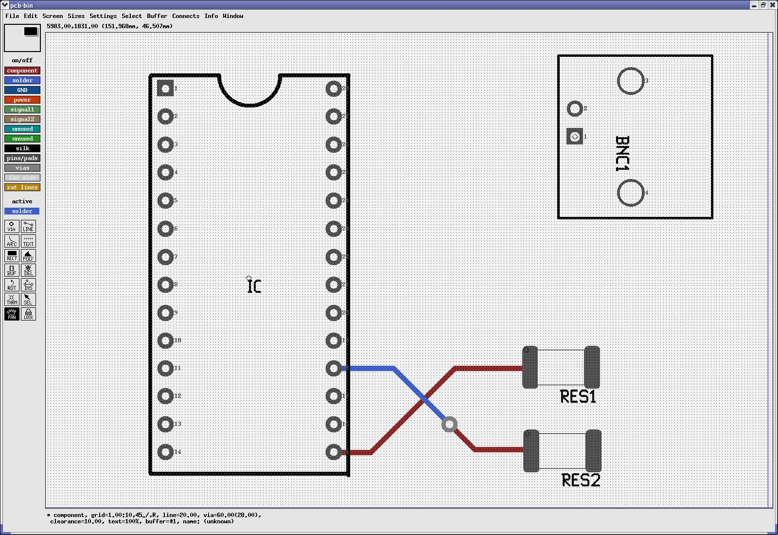
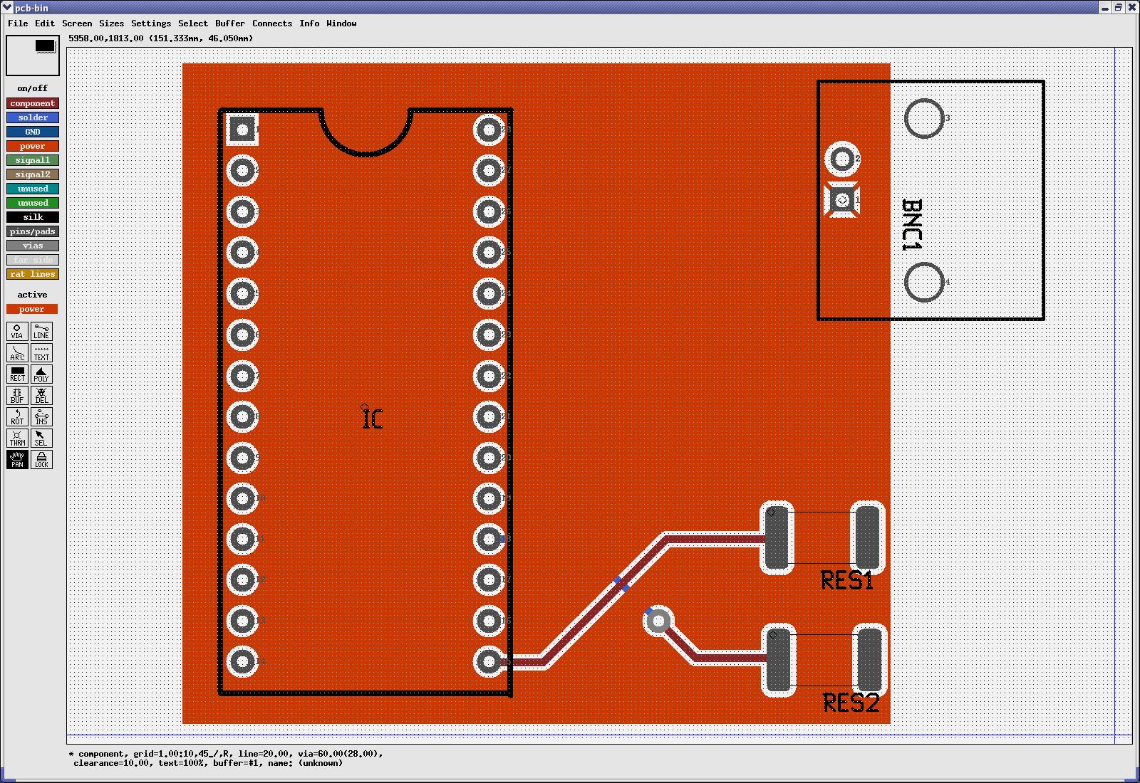
9. Now we will connect a wire from the left pad of resistor RES2
to pin 18 of the DIP. To do this, first drop a via between the
resistor pad and the previously drawn wire. Using the VIA tool on
the left to do this. Then draw a short piece of wire from the
resistor pad to the via using the component layer. Now change the
active layer to solder and
draw another wire from the via to pin 18 of the DIP. Your layout
should look similar to that shown below.
10. Often, power and ground signals are routed using a "plane"
rather than a wire. We will place the power planes on the
component side of the board and the ground plane on the solder
side. To define a power plane, select the RECT tool on the
left and make sure the active layer is set to power. Draw a power
plane that covers the components in the layout as shown below.
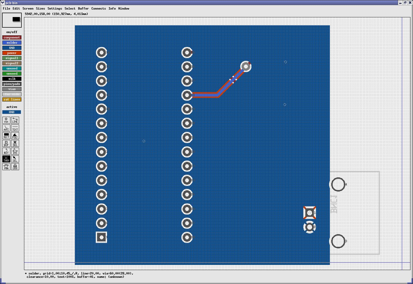
Pin 1 of the BNC connector footprint is used to route the power
signal. Therefore, we must connect this to the power plane.
Do this by selecting the THRM (thermal) tool and making sure the active
layer is still set to power.
Press the left mouse button over pin 1 of the BNC connector. Your
layout should now look as shown below.
To define a GND plane, press <TAB> to view the solder side of the
board. Then set the active layer to GND and select the RECT
tool. Draw a plane similar to that shown in the figure
below. Connect pin 2 of the BNC connector to the plane using the
THRM tool as before.
11. When we have finished laying out and connecting all the
components, we must perform a DRC check to ensure that there are no
spacing or width violations. Before doing this, go to Sizes and reduce the DRC minimum
silkwidth to 1.00. Now go to Connects
-> Design Rule Checker to
perform the DRC. The checker will stop and notify you every time
it finds a DRC violation. These errors appear in the program's
log window. Fix any DRC errors before continuing.
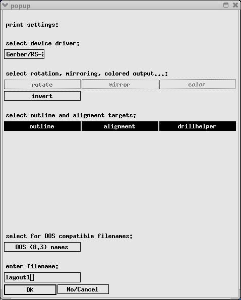
12. The PCB is fabricated by an external manufacturer. The
manufacturer receives a number of text files created by the PCB design
software that contain physical layout data. To generate these
files, go to File ->
Print Layout. Fill in
the form as shown below. In the enter
filename box, type in your directory and the name of your
layout. Hit OK when you
are done.
Additional Information
1. Most of the footprints for components you will need can be
found in the various libraries that come with PCB. If you cannot
find an appropriate footprint, you will need to make your
own. For information on how to do this, see section 8.2 on page
69 of the user's manual.
2. For a list of through-hole and surface-mount components, go to
www.digikey.com and browse through their
catalogues. These usually come with mechanical drawings from
which you can more easily make your own footprints.
3. You can use "rat" lines to logically connect pins from
different components before actually routing wires. This allows
you to optimize the placement and orientation of components without the
inconvenience of moving or deleting PCB traces. The Netlist layer is used for this
purpose. See the user's manual for more information.